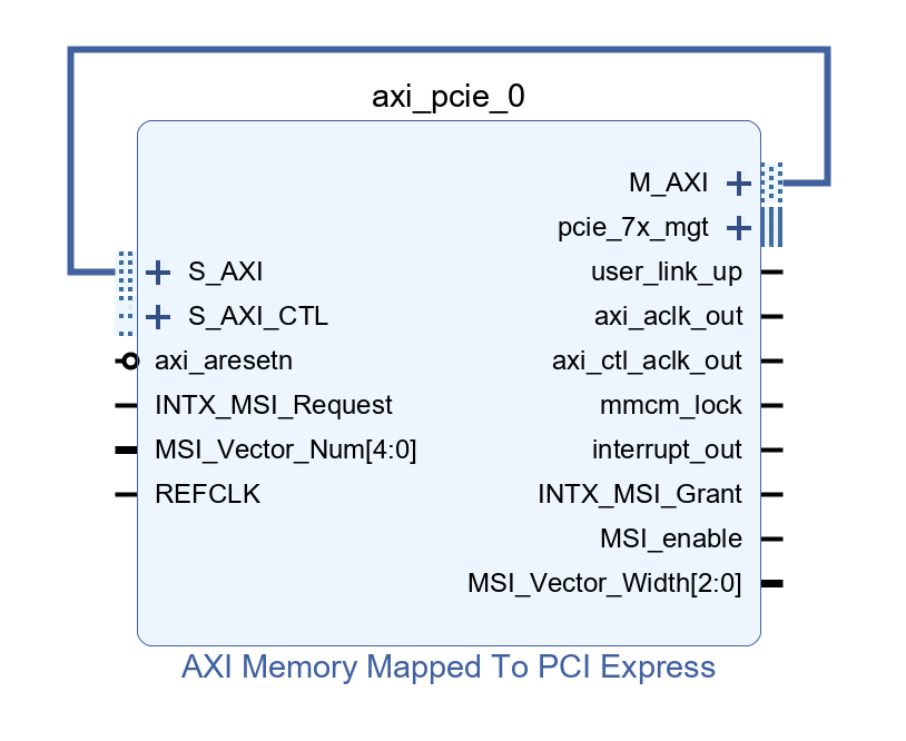
Hello, have you ever used Xilinx's AXI PCIe IP before? I directly connected the M-AXI interface of this IP to the S-AXI interface, with PCIE:BAR0 mapped to the PCIe configuration space and PCIE:BAR1 mapped to AXI:BAR0 . In the WDF driver, I created a CommonBuffer whose starting address is 16MB-aligned (because the least significant 24 bits of AXIBAR2PCIEBAR_0L are not writable and always remain 0). I wrote the aligned logical address (bus-relative address) to the AXIBAR2PCIEBAR_0L register through PCIE:BAR0 , thereby mapping AXI BAR0 to the CommonBuffer in the host memory. Subsequently, when the WDF driver writes data to PCIE:BAR1 (i.e., writing to AXI:BAR0 ), the CommonBuffer should theoretically contain the written data since AXI:BAR0 is mapped to the CommonBuffer in the host memory. However, in practice, the CommonBuffer does not receive the data. My primary goal is to perform DMA testing using the AXI PCIe IP. Is my approach feasible? I did not create a DMA transaction object because I intended to transfer data solely through the CommonBuffer.
No. You did fine up to there, but that is NOT how it works. There is no "automatic" mapping from the BAR through to the common buffer. All that register does is configure the DMA engine. When you program the on-chip DMA engine to do a transfer, you give it an AXI address. The DMA engine uses AXIBAR2PCIEBAR to translate that address to PCIE space. That's all it does. When you write to BAR1, that's just a single memory write. That does NOT automatically trigger a DMA transaction. You have to do that by hand, by writing to the PCIe IP registers.
And by "DMA transaction" there, I simply mean "a DMA action by the AXI IP block". That is unrelated to WDFDMATRANSACTION.
So, to cause the chip to do a DMA transfer, you need to write AXIBAR2PCIEBAR, then you need to write the starting AXI bus address of the transfer, and the number of bytes to transfer. Writing the byte count is what causes the DMA to occur.
Assuming the aligned logical address of the CommonBuffer in the WDF driver is 0x12000000, writing this value to AXIBAR2PCIEBAR_0L would set AXIBAR2PCIEBAR_0L = 0x12000000. In the AXI PCIe Bridge IP, if AXI:BAR0 is configured to 0xA0000000, and an AXI Master on the AXI bus (e.g., the M-AXI interface of the AXI PCIe IP) initiates an AXI write transaction with AWADDR = 0xA0345678, the corresponding PCIe address is calculated as:
PCIE Address = AXI Address - AXI:BAR0 + AXIBAR2PCIEBAR_0L.
Substituting the values:
PCIE Address = 0xA0345678 - 0xA0000000 + 0x12000000 = 0x12345678.
This address translation is automatically performed by the AXI PCIe IP internally during transaction handling.
OK, I went out and read the Xilinx document, instead of assuming this was just like previous Xilinx PCIe modules I've used.
AXIBAR2PCIEBAR_0 is used to translate AXI reads/writes to PCIe reads/writes. PCIBAR2AXIBAR_0 is used to translate PCIe writes into the BAR regions assigned by the operating system into AXI space.
So. AXI reads and writes (originated by the chip) can be translated to arbitrary PCIe addresses, like your common buffer. PCIe reads and writes (originated by the CPU) into the BAR0 region can be translated into AXI cycles
Are you saying that you configured C_AXIBAR_0 and C_PCIEBAR2AXIBAR_0 to the same AXI address, then configured C_AXIBAR2PCIEBAR_0 to your common buffer, and then tried to write into BAR0 and expected to see the result looped back to the common buffer? It's not entirely clear to me that writes coming in through the bridge should be looped back out through the bridge. It's not an unreasonable, but I wouldn't be surprised if it didn't work.
Have you asked this on the Xilinx support forums? They tend to be rather responsive, and this is not really a Windows question.
This topic was automatically closed 60 days after the last reply. New replies are no longer allowed.